In the half-century since the transistor was invented, this workhorse component of almost every electronic device has shrunk from the size of a pencil eraser to smaller than a bacterium. The miniaturization of transistors and their sister circuit components has led to an explosion of machine intelligence in countless types of devices from computers to greeting cards. Just how much smaller transistors can get is a multibillion-dollar question. Theorists have long pondered, When will the shrinkage finally be brought to a screeching halt? If components get too small, the laws of physics seem to preclude reliable transistor action.


For generations, scientists and engineers have been inventing new materials and designs for stuffing ever more circuit components into ever less space (SN: 11/25/00, p. 350: http://www.sciencenews.org/20001125/bob2.asp). Besides stuffing more functionality into gadgets, those advances also lead to faster circuitry that uses less power.
Recently, scientists have created the first experimental devices in which transistor action seems to take place in individual atoms. The results show evidence that even the elemental building blocks of matter have what it takes to be circuit components.
Electronic Lilliput
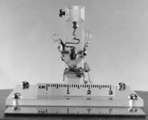
Transistors play starring roles in circuits by amplifying or otherwise converting signals. The first transistor, invented in 1947, was a centimeter-long slab of germanium pressed against the point of a triangle of plastic partly wrapped in gold foil. This device amplified an electronic signal up to 15-fold. Although early transistors were petite compared with their vacuum-tube predecessors, they didn’t shrink dramatically until the late 1950s.That’s when engineers came up with the idea of fashioning all the devices needed for a circuit–transistors, resistors, and capacitors–on a single wafer of germanium or its sister semiconductor, silicon.
Using photolithographic methods to apply circuit patterns and other processes for depositing and etching away different materials, manufacturers found they could mass-produce increasingly complex circuits on smaller and smaller flecks of semiconductor. In less than 60 years, the transistor has shrunk by a factor of roughly 10 billion. Today, Intel’s Pentium 4 microprocessor contains 55 million transistors, each averaging about 130 nanometers on a side.
Yet, chipmakers face growing difficulty using conventional deposit-and-etch technology to make even smaller components. Consequently, scientists have begun making transistors in other ways and using materials other than conventional semiconductors. Among the latter are long, electrically conductive molecules known as carbon nanotubes and ultrathin, semiconductor whiskers called nanowires (SN: 2/9/02, p. 83: Circuitry in a nanowire: Novel growth method may transform chips).
Give me a break!
Even the smallest of the nanotransistors contains thousands of atoms. Continuing to miniaturize a transistor down to just one atom requires another approach altogether. The most successful strategy so far is conceptually simple: Make an extremely fine wire, create an atom-size gap in it, and then place an atom in the gap. The result is essentially an atom flanked by a pair of electrodes. If that minuscule structure can control a current, it will be the smallest transistor possible.
Atoms come in a variety of sizes, but scientists often refer to a nominal atomic size as the diameter of the smallest, most abundant atom–hydrogen. Its diameter is about 0.1 nanometer, or a millionth the width of a human hair.
Not even the most precise deposit-and-etch fabrication method for microchips can yield wires with merely atomwide gaps in them. The best that conventional methods can muster is a break about 10 nm across. Another microfabrication technique invented in 1997 for breaking thin wires indeed can produce hydrogen-atom-wide gaps (SN: 11/8/97, p. 293: http://www.sciencenews.org/sn_arc97/11_8_97/fob2.htm), but the resulting structures are not suitable for making transistors, explains Daniel C. Ralph of Cornell University.
Three years ago, Hongkun Park, Paul L. McEuen, and their colleagues found that they could turn a major headache for electronics firms into an advantage. When large electric currents pass through narrow wires on microchips, the flowing electrons can shove some atoms along–eroding away the metal and eventually breaking the wires.
“This is a bad thing in the semiconductor industry,” notes McEuen. “Interconnects fail, and [chip manufacturers] hate it.”
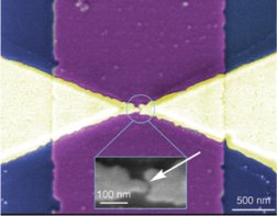
However, the researchers, who were then at the University of California, Berkeley, realized that this electromigration of atoms might offer them a delicate and precise way to create minute cracks in wires. After depositing gold wires only 10 to 15 nanometers thick on a microchip, the scientists found that driving large currents through the wires for about 2 minutes would scour away enough gold to form gaps, on average, about 1 nm across. That’s larger than an atomic diameter, but it’s in the ballpark.
By bathing the wires, either before or after creating the gaps, with a solution of molecules or a suspension of tiny semiconductor crystals, the researchers would often find that some of the gaps harbored just one molecule or nanocrystal. Once they’d mastered the technique, the researchers used it to create a wee transistor from a nanocrystal of cadmium selenide, a semiconducting compound. A year later, the team used the same method to make another transistor from the 60-carbon-atom, soccer ball–shape molecule known as a buckyball (SN: 7/13/02, p. 26: Buckymedicine).
In 1999, Park moved to Harvard University to head his own research group. Then, last year, McEuen moved his research team to Cornell University. Since Park’s departure from Berkeley, each of the separate teams has rushed to build upon the earlier, joint efforts and snare a single atom within the tiny electromigration-created gaps of their nanoscale gold wires.
This spring, the groups simultaneously reported completing the final step in wiring an atom. Independently, each team had synthesized its own custom-designed molecule that behaves like a pair of electrical leads dangling from a central atom or atoms. Plugging such a molecule into the gap of gold nanowire provides the last electrical link needed to create an atomic transistor.
McEuen, Ralph, and their colleagues at Cornell and Berkeley describe their new transistor, whose central player is a cobalt atom, in the June 13 Nature. In the same issue, a second report describes similar work by Park and his colleagues at both Harvard and Berkeley. However, the transistor action in this case relies on two vanadium atoms, not one cobalt atom.
“This is amazing physics, and it’s very cleverly and expertly revealed by both these papers,” says James C. Ellenbogen of the Mitre Corporation in McLean, Va. However, he balks at labeling the new transistors as atomic-scale devices. After all, he notes, the active atoms are bound within molecules that contain dozens of atoms.
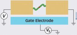
As with their previous nanoscale transistors, McEuen, Park, and their coworkers control current in the new devices by means of voltages applied to so-called gate electrodes. In these transistors, the gate electrodes lie beneath the metal-containing molecules.
Both teams recently demonstrated that changing the voltage on a gate electrode alters the electron-energy levels of the overlying molecule’s metal atoms. In a complex way, those alterations make it easier or harder for electrons to hop from a side of the broken gold wire onto the atom or atoms inside of the gap. Likewise, the gate-voltage changes affect how readily electrons hop off the atoms to the segment of the wire on the other side of the gap. In this way, the gate voltage regulates the flow of electrons through the device. Such control of current by means of a voltage is a hallmark of transistors.
McEuen describes the general molecular structure of the new molecules as “a little, tiny piece of metal embedded inside an insulator.” The nonmetal portions contain carbon and have end groups that readily bind to gold electrodes. The teams designed their tethers to be poor electrical conductors to encourage the electrons to move to the metal atoms.
The new molecules belong to a group of structures, known as metal coordination complexes, that are common in nature and well known to chemists, notes McEuen. Hemoglobin, for instance, is an iron-based complex that ferries oxygen in blood. Other metal coordination complexes play a role in photosynthesis.
It was a fortunate combination of chemists’ familiarity with such complexes and physicists’ experience with tiny structures governing electron behavior that led to the unprecedented reduction in transistor size, McEuen says.
One small step
Achieving transistor behavior in an atom is a far cry from actually squeezing a transistor into the space of an atom. Researchers have yet to clear that second miniaturization hurdle.
As with all molecular-scale electronic devices made to date, scientists lack the means to connect those components to each other or to the outer world–for instance, to measuring instruments–with wiring as miniature as the devices themselves. The electrodes that carry current to the atoms actually doing the work in the new experiments occupy millions of times as much area as the central atoms do.
Still, other obstacles loom in the practical implementation of atomic-scale transistors. The current devices, for example, operate only at temperatures approaching absolute zero. At warmer temperatures, the molecules start writhing around too much to support reliable transistor action, Ralph explains.
Whether they lead to anything practical or not, the new devices provide a welcome opportunity for researchers to learn more about electron behavior on nanometer scales, says Leo P. Kouwenhoven of the Delft University of Technology in The Netherlands. For more than a decade, scientists have been observing the antics of electrons confined within so-called quantum dots. These are usually nanoclusters of semiconductor atoms (SN: 6/17/00, p. 392) or tiny regions of a microchip that can confine electrons like boxes would (SN: 4/11/98, p. 236). Researchers have manipulated such dots to create lasers, fluorescent markers for biomolecules, and single-electron transistors in which current flows only one electron at a time.
These dots are so small that quantum mechanics determines their characteristics–for instance, the energy levels of the electrons inside them and how electrons pass in and out of the structures. Even smaller, however, are the newly developed atomic-scale transistors. They represent “the ultimate limit” for quantum dots, McEuen says.
Like their larger cousin dots, the atomic-scale transistors exhibit curious electron behaviors, including currents made of electrons moving single file and a phenomenon called the Kondo effect. Generally, in materials being cooled to near absolute zero, the Kondo effect–named after the Japanese theorist who explained it in 1964–appears as a sharp rise in electrical resistance below a certain temperature if small amounts of a magnetic substance are present.
In quantum dots, however, the effect shows an opposite face: Resistance fades when the temperature drops below a so-called Kondo temperature. Because the effect boosts the current-carrying capacity of single-atom transistors, it increases the practicality of these as components for computers or other devices, says David Goldhaber-Gordon of Stanford University.
However, Goldhaber-Gordon doubts that atomic-scale transistors will ever displace silicon. They may someday lead instead to exceptionally dense memory units that might occupy spaces between conventional components on a microchip.
For the time being, atomic-scale transistors remain a laboratory curiosity, at least until researchers can push them further. Toward that end, McEuen and his group now are planning to wire atom transistors together using carbon nanotubes.
Even better, suggests Kouwenhoven, would be to develop macromolecules that incorporate all the needed circuit elements–transistors, resistors, and capacitors–as do today’s integrated circuits. If that becomes possible, a poppy seed–size speck of such macromolecules could pack the digital power of a supercomputer.


